Robotics Blog
The Future of CMOS Sensors
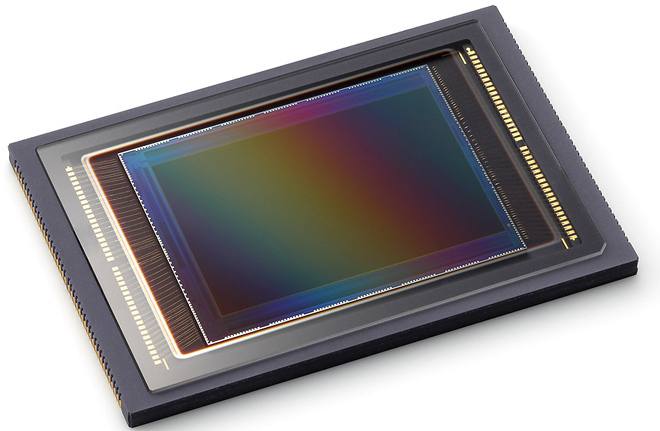 Over the last few years, one industry has driven the most demand for CMOS image sensors: Cell phones.
Cell phones have come a long way in the last decade, going from grainy still shots to crisp and clear photos and videos. It’s no surprise that machine vision and other industries that rely on imaging technology have also benefited from this surge.
As we move into 2017, the mobile market will pass the torch to new high-volume applications.
Industries including automotive, healthcare, and even virtual reality will begin to dictate imaging development. At the same time, the range of innovation in image capture for consumer products like cell phones and tablets will get narrower.
Tomorrow’s CMOS Market Transformed by New Ideas
Several industries that once had limited or, indeed, no use for image capture are now serving as engines of innovation. Even if the consumer mobile market reaches saturation or contracts, image sensor technology can still be expected to enjoy consistent evolution.
Some new frontiers in imaging include:
Automotive
Recently, interest in safety features requiring image capture has intensified. Rear-view visibility systems now make it possible for drivers to prevent many potentially serious accidents. Driver assistance systems use imaging to avert collisions and facilitate lane change.
Thermal Infrared Imaging
The ability to see beyond the visible spectrum has many applications in health and safety. With infrared property surveillance, intruders can be easily detected at night. Used with autonomous aerial vehicles, thermal infrared imaging has shown great promise in search and rescue.
Certified System Integrator Program
Set Yourself at the Forefront of the Global Vision Market
.jpg) Vision system integrators certified by A3 are acknowledged globally throughout the industry as an elite group of accomplished, highly skilled and trusted professionals. You’ll be able to leverage your certification to enhance your competitiveness and expand your opportunities.
Vision system integrators certified by A3 are acknowledged globally throughout the industry as an elite group of accomplished, highly skilled and trusted professionals. You’ll be able to leverage your certification to enhance your competitiveness and expand your opportunities.
Spectroscopy and Hyperspectral Imaging
Machine vision experts are increasingly experimenting with the commercialization opportunities of imaging focused on advanced material differentiation. By recognizing an object’s reflectivity and absorption properties, it may be possible to detect harmful bacteria and other toxins.
Cheaper and Lighter Lenses Will Enhance Imaging Everywhere
As foundational lens technology becomes lighter and less expensive, all forms of imaging are sure to benefit. Researchers at Caltech have recently made a breakthrough that could spark widespread adoption of cutting-edge flat optical lenses.
By stacking two metasurfaces, sheets of metal with adjustable electromagnetic properties, the Caltech team developed lens that don’t exhibit the classical curved shape. Tens of millions of “nanoposts,” silicon cylinders 600 nanometers tall, are arranged on each metasurface.
Since the nanoposts can have varying diameters, engineers can fine-tune the path of light passing through them and thus generate remarkable flat lenses. They can easily be integrated with CMOS image sensors, since they use the same manufacturing techniques and materials.
Flat lenses have the potential to transform consumer and industrial imaging as we know it – but that’s not all. They can also be used at much smaller scales than today’s lenses, leading to novel medical applications as well.
Recent Posts
- How 3D Vision Systems Are Transforming Food Manufacturing
- Autonomous Driving Technology: Dueling Approaches Fight for Control of the Wheel
- These Farms Are Harnessing Machine Vision for Smarter Agriculture
- Revealing the Hidden Effects of Climate Change with Advanced Imaging
- Innovative Machine Vision Lenses and Trends
- An Early Look at GigE Vision 3.0
- View All Robotics Blogs