Vision & Imaging Blog
Detecting Defects With 2D & 3D Automated Optical Inspection
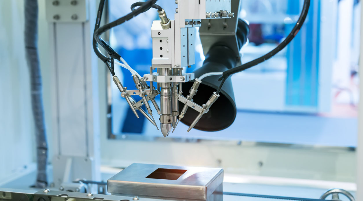 The miniaturization trend in packaging has led to increased printed circuit board (PCB) density and complexity. Because boards are more complicated, there is a higher probability for defects to occur on finished PCBs. Automated Optical Inspection (AOI) scans PCBs for both catastrophic failure and quality defects.
AOI is often used in the manufacturing process because it’s a non-contact test method. It has primarily been used after solder reflow or in post-production. Post-reflow AOI systems inspect for many kinds of defects, including component placement issues, solder shorts, or missing solder. Faulty boards can be reworked and acceptable boards are sent to the next stage.
Detecting Defects with AOI Systems
Some AOI systems check a specific task, such as paste, pre-reflow, or post-reflow. AOI cost is justifiable if manufacturers spend a lot of time inspecting. AOI machines are fast and reliable. They can notify of problems that occur repetitively. And they can track main problems and help improve manufacturing processes.
AOIs inspect the following, among others:
- Area defects
- Component offset
- Component presence or absence
- Component skew
- Excessive solder joints
- Flipped component
- Insufficient solder joints
- Presence of foreign material
- Severely damaged components
- Wrong part
Need for AOI Advancement
The AOI industry has long relied on 2D inspection principles to test workmanship quality. This technology is suitable for detecting many defects. But ultraminiature chips, leaded devices, and LED packages make a 3D inspection technology necessary. However, there are advantages and limtations to both technologies. Therefore, AOI systems are most efficient if they employ both 2D and 3D inspection technology.
ROI Calculator

Discover the potential cost savings of robotic automation over a 20-year system life
This calculator compares your current manual labor costs against the total cost of owning and operating a robotic system over its 20-year lifespan.
2D AOI Systems
2D inspection technology is the most common solution in use. The most advanced systems have multiple high-resolution cameras, 10 to 15 MP resolution, and precise lenses. They also use sophisticated inspection algorithms to inspect for defects.
Advantages of 2D Systems:
- Mature technology
- Cost-effective
- High speed
- Less susceptible to shadowing issues
- Able to inspect tall devices > 5mm
- Flexible inspection capabilities
Limitations of 2D Systems:
- Not capable of true-co-planarity inspection
- Can’t provide volumetric measurement data
- Increased false call rate
3D AOI Systems
3D inspection tech has existed for many years, but it’s typically only been used to inspect solder paste deposition on PCDs right after the screen-printing process. But 3D inspection has recently been added to other areas. Laser measurement is used to provide a 3D measurement of height sensitive devices. This method helps detect co-planarity defects that may be missed with 2D inspection methods.
Advantages of 3D Systems:
- True co-planarity inspection capability
- Volumetric inspection data
- Reduced false call rate
Limitations of 3D Systems:
- Emerging technology
- Incapable of inspecting 2D elements
- Significant cost increase
- Significant reduction in speed
- Height limitation, about 5mm max
- Shadowing issues
- No color inspection
2D AOI has long been relied on for testing and inspection of defects. However, with the unique inspection needs of ultraminiature chips, leaded devices, and LED packages, 3D inspection technology is also necessary. Manufacturers are now able to leverage both 2D and 3D AOI to offset the limitations of each to meet more of their testing and inspection requirements.
Share This On X:
The downsizing of packaging has led to more complex and dense printed circuit boards (PCBs). Since PCBs have become much more complex, inspection processes can help avoid catastrophic failures and quality defects.
Automated Optical Inspections (AOI) can help reduce quality defects and failures in highly complex printed circuit boards. #machinevision
Recent Posts
- How 3D Vision Systems Are Transforming Food Manufacturing
- Autonomous Driving Technology: Dueling Approaches Fight for Control of the Wheel
- These Farms Are Harnessing Machine Vision for Smarter Agriculture
- Revealing the Hidden Effects of Climate Change with Advanced Imaging
- How Vision Systems Are Transforming Predictive Neurodiagnostics
- Innovative Machine Vision Lenses and Trends
- View All Vision & Imaging Blogs