PI (Physik Instrumente) LP Product
Member Since 2017
PI is a leading manufacturer of precision motion control and automation systems, hexapod 6-axis parallel robotic stages, air bearing motion systems, Gantry Systems, 3D printing, laser machining, and piezoelectric nano-positioning solutions. Applications include photonics, semiconductor technology, medical engineering, assembly, inspection,
Product filed under:
Metrology Machinery / Equipment, Positioning Slides / Linear Units, and Power Transmission Metrology Machinery / Equipment, Positioning Slides / Linear Units, Power Transmission, and Actuators & Mechanics
See More
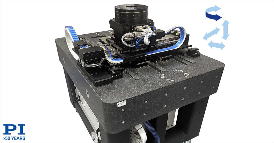
Wafer Stages for Glass Substrate Inspection and Semiconductor Metrology
Model: Wafer Stages
High precision, engineered motion systems for semiconductor metrology and the automation, inspection and lithography applications.
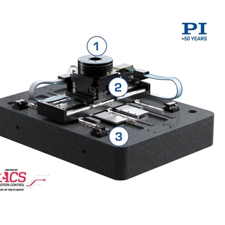
PI, a global leader in nanopositioning, high precision motion control and automation provides engineered, granite-based multi-axis precision motion systems for the semiconductor industry These systems are designed for the automation of wafer metrology, glass substrate inspection and lithography applications. These highly accurate stages are based on modular concepts that allow fast customizations. Several technologies are available including air bearings, rails-on-granite, and several types of piezo drive systems. Large travel ranges of one meter and more can be achieved with a variety of different configurations. The XYZ-Theta example wafer stage shown is designed for thin film metrology equipped with direct drive motors, nanometer resolution encoders, and high-performance ACS motion controllers
PI’s advanced design expertise and long experience as a supplier to top tier semiconductor manufacturers and leading system integrators enables us to understand and meet the high demands of the industry, including copy exactly and meeting strict cleanroom requirements.
More information on precision motion for semiconductor applications
Other Products from PI (Physik Instrumente) LP
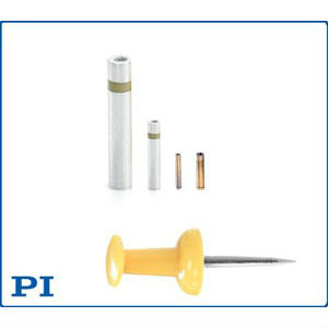
Piezoelectric Transducers, Piezo Micro-Tubes
High Performance Miniature Piezoelectric Transducers, Piezo Micro-Tubes