What Is the Difference Between CCD and CMOS Sensors?
CCD (Charge-Coupled Device) and CMOS (Complementary Metal-Oxide-Semiconductor) are the two main sensor technologies used in machine vision and digital cameras, differing fundamentally in how they capture light and read out image data. CCD sensors transfer charge sequentially from pixel to pixel for centralized conversion to voltage, while CMOS sensors convert charge to voltage at each pixel with integrated amplification and readout circuitry.
CCD technology dominated industrial imaging for decades due to superior image quality, uniformity, and low noise. CMOS sensors initially suffered from higher noise and fixed pattern artifacts but have improved dramatically through advanced fabrication processes. Modern CMOS sensors now match or exceed CCD performance in most metrics while offering significant advantages in power consumption, integration, and cost. The industry has largely transitioned to CMOS technology, with CCD production declining as manufacturers discontinue legacy models. However, understanding both technologies remains important since existing CCD-based systems continue operating in many facilities, and some specialized applications still benefit from CCD characteristics.
Why Has the Industry Shifted From CCD to CMOS?
The machine vision industry shifted from CCD to CMOS sensors due to CMOS advantages in power consumption, on-chip integration, manufacturing cost, and continuous technology advancement, while CMOS image quality improved to match CCD performance for most applications.
Power Efficiency
CCD sensors require multiple voltage levels (often 3-5 different voltages) and relatively high power for charge transfer across the sensor. A typical CCD camera might consume 5-10 watts, requiring active cooling or substantial heat sinking. The sequential charge transfer process is inherently power-intensive as charge packets move through many stages.
CMOS sensors operate on single low-voltage supplies (1.8-3.3V) with power consumption proportional to pixel readout rate. Modern CMOS cameras consume 1-3 watts for equivalent resolution and frame rate, often requiring no active cooling. Lower power enables compact camera designs, reduces cooling requirements, and allows battery operation for mobile applications.
On-Chip Integration
CMOS manufacturing processes allow integrating camera functions directly on the sensor chip. Analog-to-digital converters, timing generators, image processing, and even specialized functions like region-of-interest readout or multi-exposure HDR processing can be integrated on the sensor itself.
CCD sensors require separate chips for these functions, increasing camera complexity, board space, and manufacturing cost. A CMOS camera-on-a-chip contains functionality requiring multiple circuit boards in equivalent CCD cameras, enabling much more compact camera designs.
Manufacturing Economics
CMOS sensors are manufactured using standard semiconductor fabrication processes shared with logic chips, microprocessors, and memory. This allows leveraging massive fabrication capacity and ongoing process improvements driven by the broader semiconductor industry. CCD production requires specialized processes unique to imaging, limiting economies of scale.
As semiconductor fabs advanced to smaller process nodes for logic and memory, CMOS sensor manufacturers benefited from improved pixel performance, lower costs, and access to cutting-edge fabrication technology. CCD technology improvements slowed as specialized CCD fab capacity declined and investment shifted to CMOS development.
Performance Convergence
- Global shutter CMOS eliminated rolling shutter limitations in motion applications
- Back-side illuminated (BSI) technology improved quantum efficiency to match or exceed CCD levels
- Advanced noise reduction techniques brought read noise to CCD-equivalent levels
Market and Strategic Factors
Major sensor manufacturers discontinued CCD product lines to focus resources on CMOS development. This created uncertainty about long-term CCD availability, prompting camera manufacturers and end users to transition to CMOS platforms for new designs. The virtuous cycle of increased CMOS development leading to better performance and lower costs accelerated the transition.
How Do CCD and CMOS Compare in Noise and Quantum Efficiency?
Modern CMOS sensors achieve read noise levels of 1-3 electrons RMS and quantum efficiency above 60%, matching or exceeding CCD performance that typically shows 2-5 electrons read noise and 50-70% quantum efficiency, with differences narrowing as CMOS technology advances.
Read Noise Comparison
Read noise represents the uncertainty in measuring the signal from each pixel, expressed in electrons RMS. Lower read noise enables detection of dimmer signals and improves dynamic range. High-quality CCD sensors achieve 2-5 electrons RMS read noise using sophisticated output amplifiers and low-noise readout techniques.
Early CMOS sensors exhibited 10-20 electrons read noise due to pixel-level amplification variations and less optimized readout circuitry. Modern CMOS sensors with advanced pixel designs and column-level signal processing achieve 1-3 electrons read noise, effectively matching CCD performance. Scientific CMOS (sCMOS) sensors designed for research applications reach sub-electron read noise levels using specialized readout architectures, actually surpassing most CCDs in this metric.
Quantum Efficiency
Quantum efficiency measures what percentage of incident photons are converted to detectable electrons. Higher quantum efficiency means better sensitivity and ability to detect dim features. CCDs traditionally achieved 50-70% quantum efficiency across visible wavelengths, with specialized sensors reaching 80-90% through optimization.
Front-side illuminated CMOS sensors initially showed lower quantum efficiency (40-60%) because pixel circuitry blocked some light from reaching the photodiode. Back-side illuminated (BSI) CMOS technology flips the sensor so light enters from the back, avoiding circuitry obstruction and achieving 70-85% quantum efficiency, matching or exceeding CCD performance. For near-infrared wavelengths used in many inspection applications, modern CMOS sensors often exceed CCD quantum efficiency due to silicon thickness optimization and anti-reflective coating improvements.
Dark Current
Dark current is the signal generated without illumination due to thermal effects. CCDs generally show lower dark current than CMOS sensors at equivalent temperatures, an advantage for extended exposures in scientific imaging. However, for typical machine vision applications with millisecond exposure times, dark current contributes negligibly to total noise for both technologies. Active cooling can reduce CMOS dark current to levels acceptable even for second-long exposures when required.
Uniformity and Fixed Pattern Noise
CCDs excel in pixel-to-pixel uniformity since all pixels use identical readout paths and a single output amplifier. This produces very low fixed pattern noise, making CCDs attractive for applications requiring flat-field correction or precise intensity measurements across the image.
CMOS sensors with per-pixel amplification show higher fixed pattern noise from pixel-to-pixel gain variations. Column-level processing and calibration during manufacturing reduce this effect substantially, and modern CMOS sensors achieve uniformity adequate for most machine vision applications. Applications requiring extreme uniformity may still prefer CCD technology where available.
Which Sensor Type Is Best for High-Speed or Low-Light Imaging?
CMOS sensors are better for high-speed imaging due to faster readout architectures and lower power consumption enabling compact high-frame-rate cameras, while low-light imaging depends on specific requirements, with modern CMOS matching CCD sensitivity for most applications and scientific CMOS exceeding CCD performance.
CCD vs CMOS: Feature Comparison
| Feature | CCD Sensors | CMOS Sensors |
|---|---|---|
| Read Noise | 2-5 electrons RMS (typical) | 1-3 electrons RMS (modern sensors) |
| Quantum Efficiency | 50-70% (front-illuminated), up to 90% (optimized) | 40-60% (front-illuminated), 70-85% (back-side illuminated) |
| Readout Speed | Moderate, limited by sequential charge transfer | Fast, parallel readout architecture |
| Power Consumption | 5-10W typical | 1-3W typical |
| Dynamic Range | 60-70 dB typical | 60-75 dB (modern sensors) |
| Fill Factor | 100% (full-frame CCD) | 70-90% depending on pixel architecture |
| On-Chip Functions | Limited, requires external circuitry | Extensive, ADC and processing on-chip |
| Cost | Higher due to specialized manufacturing | Lower, standard semiconductor processes |
| Availability | Declining, legacy products | Wide selection, active development |
| Best For | Legacy systems, extreme uniformity requirements | New designs, high-speed, integration requirements |
High-Speed Imaging Advantages
CMOS sensors dominate high-speed imaging due to their parallel readout architecture. While CCDs must sequentially transfer charge row by row to output amplifiers, CMOS sensors can read multiple rows or columns simultaneously. This enables frame rates of 100-1000+ fps for multi-megapixel sensors.
The lower power consumption becomes critical at high frame rates. A CMOS camera running at 500 fps might consume 3-4 watts, while an equivalent CCD camera would require 15-20 watts, necessitating substantial cooling that adds size, weight, and complexity. Region-of-interest readout, available on many CMOS sensors, further increases frame rates by reading only relevant image areas. A 4-megapixel CMOS sensor might run at 200 fps full-frame but achieve 2000 fps reading a 640x480 ROI.
Low-Light Performance
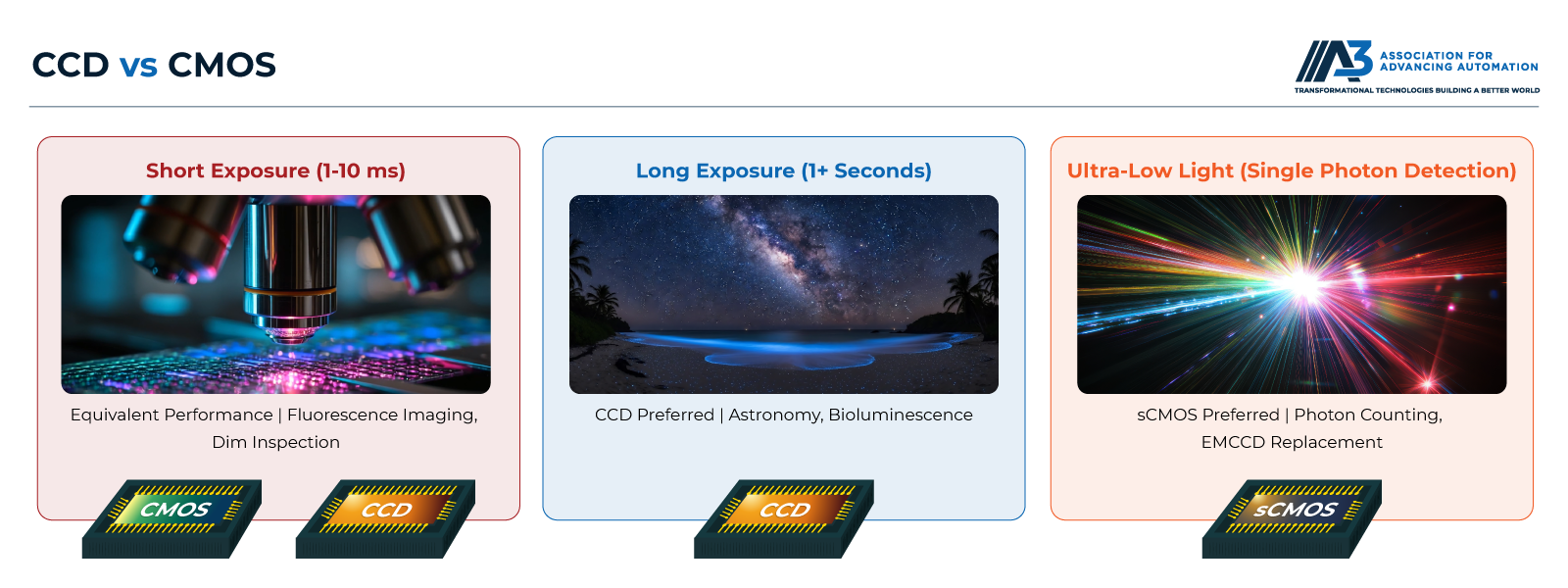
Short Exposures (1-10ms): Modern CMOS sensors with low read noise and high quantum efficiency perform equivalently to CCDs. Applications like fluorescence imaging, dim parts inspection under controlled lighting, or low-light tracking benefit equally from either technology when selecting modern high-performance sensors.
Long Exposures (1+ seconds): CCD sensors generally show lower dark current, providing cleaner images in long exposures. Astronomy, bioluminescence imaging, and scientific applications requiring extended integration times may prefer CCD technology where available, though cooled CMOS sensors can achieve comparable performance.
Ultra-Low Light (single photon detection): Specialized CMOS sensors with electron multiplication or photon-counting capabilities now match or exceed CCD performance. Scientific CMOS (sCMOS) technology enables ultra-low light imaging previously requiring expensive electron-multiplying CCDs (EMCCDs).
Application-Specific Recommendations
Manufacturing Inspection: CMOS sensors provide better overall value with adequate image quality, lower power, and faster frame rates. Most new inspection systems use CMOS cameras.
Robotics and Automation: CMOS sensors' compact size, low power, and high-speed capabilities make them the clear choice. Integration of image processing on-chip enables smart cameras ideal for robotic vision.
Scientific Research: Application-dependent. Astronomy and long-exposure spectroscopy might prefer cooled CCDs for lower dark current. High-speed cellular imaging, neuroscience, and modern microscopy techniques increasingly use sCMOS sensors for superior speed and sensitivity combinations.
Legacy System Support: Facilities with existing CCD-based systems must consider parts availability. If CCDs become unavailable, system redesign around CMOS cameras may be necessary, potentially requiring significant software and integration work.
Conclusion
The transition from CCD to CMOS sensors reflects CMOS technology's evolution from early inferior performance to current superiority in most metrics relevant to machine vision and industrial imaging. CMOS advantages in power efficiency, integration, manufacturing cost, and continuous development make it the technology of choice for new camera designs.
Modern CMOS sensors match CCD image quality for noise, quantum efficiency, and dynamic range while offering significant advantages in readout speed, power consumption, and on-chip functionality. The declining availability of CCD sensors as manufacturers discontinue production reinforces the industry shift to CMOS platforms.
For new machine vision systems, CMOS sensors are the clear choice unless specific requirements demand characteristics only available in specialized CCD sensors. Understanding both technologies remains valuable for maintaining existing systems and appreciating the technical evolution that has shaped modern industrial imaging.
Recommended Resources
Explore more vision and imaging insights
CCD vs CMOS Image Sensors: Which are Better?
When considering different designs in an imaging system, one of the major decisions to be made is whether you should use a CCD image sensor or a CMOS image sensor. The rest of your imaging system will revolve around this choice, as will the resulting performance of the imaging system.
Spark Series SP-20000 CMOS Camera Now Has CoaXPress and USB3 Vision Interface Options
JAI today added two new interface options to its 20-megapixel CMOS camera family. The Spark Series SP-20000 cameras have previously only been available with a power-over-Mini-Camera...
Ace USB 3.0 Cameras with 2 MP and 4 MP CMOS Sensors
Camera manufacturer Basler is expanding its portfolio of ace USB 3.0 cameras to models featuring 2 MP and 4 MP CMOS sensors CMV2000 and CMV4000 from CMOSIS. The cameras are available in monochrome and color as well as in near-infrared.