Industry Insights
Metrology + Intelligence = Modern Machine Vision
“To me, metrology means the inspection of surface composition, structures and materials,” says Markus Tarin, President and Founder of MoviMED (Irvine, California). “Metrology isn’t specific to machine vision. 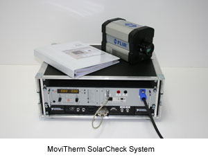 Machine vision metrology is more about quantifiable measurements and analysis of structures. It often includes 3D depth measurements, and can go beyond the traditional ‘camera’ machine vision approach. We commonly use confocal microscopy, light scatter techniques and chromatic aberration sensors in our machine vision metrology systems.”
“We’re talking large area, high-resolution inspection in flat panels, for instance, where they have to inspect every millimeter for cracks and scratches in a 2-meter square piece of glass,” explains Ben Dawson, Director of Strategic Development, Teledyne DALSA Inc. (Billerica, Massachusetts). In automotive applications, it’s about dimensioning, holding a 2.5 micron tolerance, and in pharmaceuticals, measuring the thickness of a coating on a pill…this is where metrologists really shine.”
Adding Intelligence to Metrology
While machine vision metrology systems can be found in many industries, from surgery to metal manufacturing, some of today’s hottest metrology applications by unit and sales volume are solar cell inspection and flat panel (TV) glass inspection. Both applications require the machine vision system to find defects as small as a few microns on very large areas measuring meters per side.
“It’s a special animal when it comes to these types of applications,” says Tarin. “Sometimes it means meeting resolution requirements that go beyond what traditional visible light solutions can do because you’re trying to get down to hundreds of a nanometer. You need to have special confocal microscopy solutions or other methods to get below the optical resolution limit of conventional camera based systems.”
For example, MoviMED offers a system that measures chromatic aberration using a polychromatic white light source. It measures how different wavelengths within the visible spectrum reflect from the object based on differences in the refractive index of two materials, such as a translucent coating on a pill. “Typical machine vision algorithms don’t really apply here because you’re looking at textures and structures with depth measurement and roughness measurements, which are typically the domain of scientific imaging,” adds Tarin. “The challenges become a whole lot more complex for these applications.”
When it comes to solar cell and flat panel inspection, machine vision solutions adapt their methods to meet the unique requirements of these applications too. For instance, creating an image of a 2 meter-square glass panel with micron resolution could create image files in the terabytes. This is where machine vision excels over traditional metrology solutions because the systems use application experience and intelligence to reduce the resulting data files to manageable levels.
Line scan cameras are the sensors of choice for several reasons. High-resolution line scan cameras are cheaper than area arrays of the same width, and can also produce higher quality images.
“Some people will think best way to do a high-resolution inspection is to use an area scan camera, taking 12 megapixel images per frame. But to build a sensor that size that is completely free of defects at a reasonable cost is almost impossible,” explains Teledyne DALSA’s Dawson. “It’s much easier to guarantee that a line scan camera has perfect pixels.”
By using multiple CCD line scan sensors in a TDI configuration, manufacturers can run their production lines faster or find smaller defects. A TDI camera combines the signal from multiple exposures of TDI stages for higher-speed, high-resolution applications in charge domain, rather than voltage, increasing the signal while keeping the noise floor relatively constant, yielding brighter images in low-light environments, according to Xing-Fei He, Senior Product Manager of Teledyne DALSA.
“When you do microcrack inspections, which can be as small as a few microns, the cracks are very difficult to see with visible light because it’s near the optical limit. So people will use back lighting with near infrared lights, for instance, with LED around 1 micron,” explains Xing-Fei He. “That’s a challenge for CCD because silicon has a band gap around 1.1 microns. So the quantum efficiency of silicon sensors at this wavelength is very low. By accumulating multiple exposures using multiple line TDI cameras, you can accumulate the charges in the charge domain, and really improve the signal to noise ratio.”
Tarin’s SolarCheck system uses a different, thermal lock-in approach to find very small defects on solar panels at high speeds. The solar panels are either optically or electrically excited, causing the active areas to generate a faint optical signal as well as a thermal signal. “In addition to performing an emission analysis, where we excite the cell and measure the inherent near infrared emission between 0.9 and 1.7 microns, we can also perform a shunt detection using a thermal camera with a detector that is sensitive either in the midwave IR (MWIR) region from 3µm to 5µm or in the longwave IR (LWIR) region from 8µm to 14µm. Rather than using a silicon camera without a NIR filter, we use an InGaAs detector with higher sensitivity in the NIR. Our system can perform lock-in measurements independent of the camera connected to it. Using a Lock-in technique enables our system to extract signals below the noise floor of the camera. The concept is based on the random distribution of noise combined with a known excitation signal with respect to its frequency and phase relation. A very steep band pass filter matched to the frequency of the excitation signal assures that the system only amplifies signals matching that frequency, therefore cancelling out noise. A fast-Fourier Transform then extracts phase and amplitude information from the signal. The larger the phase shift, the more contrast we assign to the pixel. Mapping the pixel-by-pixel generated phase information to the amplitude image allows the spatial location of defects, such as shunts.”
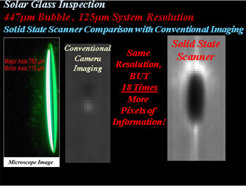
Solar cell inspection specialists, Dark Field Technologies, are in the process of patenting another approach that reportedly yields pixel imaging up to 20x of the sensors optical resolution. Dark Field Technologies focuses on thin-film solar cell inspection. The new system, called Solid State Scanning, uses a combination of white light and coherent light in a dark field imaging system, which means the optical illumination is off axis and does not normally reflect directly back to the camera.
“Fundamentally, it’s creating well-defined illumination and measuring how much scatter we get around the core,” explains Timothy Potts, President of Dark Field Technologies. “Defects, such as scratches, scatter light. The new system, which uses a DALSA Piranha2, 8k pixel line scan cameras has a unique dark field optical configuration that is self-aligning, and can detect defects down to a few microns regardless of panel warpage or vibration at speeds of 30 meters per minute. No one believes it, until they see it. And then they all buy it.”
As Dark Field, SolarCheck and other systems clearly illustrate, a great strength of machine vision is its flexibility to adapt to changing manufacturing processes and demands while using any and all optical methods available. While machine vision will never take the place of an offline Mitutoyo CMM system for accuracy and spatial resolution; working together, machine vision and quality control departments allow manufacturers to continually push the envelop of their product designs while keeping a close eye on yields and the bottom line.
AIA
AIA - Advancing Vision + Imaging has transformed into the Association for Advancing Automation, the leading global automation trade association of the vision + imaging, robotics, motion control, and industrial AI industries.
Discover how AIA can support your automation journey with their complete range of solutions and expertise.
Visit Company Website
AIA - Advancing Vision + Imaging has transformed into the Association for Advancing Automation, the leading global automation trade association of the vision + imaging, robotics, motion control, and industrial AI industries.