Industry Insights
Medical, Microscopy, and Microprocessors: Size Really Does Matter
When it comes to medical, microscopy, and microprocessors, bigger pixels give you more bang for your buck.
Medical imaging - aka x-rays - microscopy, and microprocessors may seem to be three very different applications when it comes to machine vision, but they do share one common element: all three systems are light starved.
Machine vision systems are used to being on tight light budgets. For instance, almost every time an 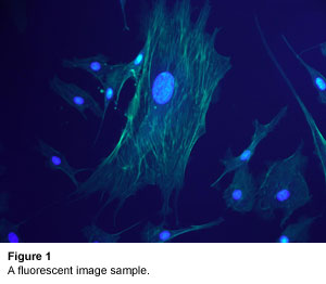 integrator solves an industrial inspection system, the client comes back with the inevitable question: “Great, but can you do it faster so I can make more money without charging me more in the bargain?”
As the speed of an inspection task increases, it shortens the available exposure time, which limits the number of photons available to generate an electrical signal inside the sensor. But exposure times aren’t the only factor that can impact the number of available photons. Unlike traditional machine vision industrial applications that capture reflected light, x-ray and microscope-based vision systems - whether they’re imaging biologics in medical research or inorganics as part of microprocessor inspection - often capture photons emitted by target materials through fluorescence and electroluminescence. Fluorescent and electroluminescent materials, such as chemical tags called fluorophores, emit light in response to optical or electrical excitation rather than reflecting light. In response, low-light cameras follow a different product development path than their traditional imaging counterparts. In other words, instead of shrinking pixels and increasing the size of sensor arrays to generate larger images with greater spatial detail, low-light cameras increase pixel size, cooling, and low-dark-noise electronics to convert the few available photons to electrons - usually at the sacrifice of spatial resolution. When it comes to fluorescence and electroluminescence in medical and microscopy applications, size really does matter.
Lower Dose X-rays
X-rays are the most common form of medical imaging. Traditionally, radiographs - or x-ray images of materials and people - were film based. X-rays passed through the subject, and were absorbed by special chemicals deposited on film to create an image. The process was slow because the film had to be developed and shipped to doctors for viewing, expensive because of the need for developing materials, and hazardous because of the special chemicals involved.
Digital radiography solved many of these problems. Today, there are two main approaches to digital radiography; the new phosphor coated large-area flat panel silicon detector, and the traditional approach of combining an image intensifier with a CCD sensor. Flat panel silicon detectors are specialized sensors that are much larger in size than a machine vision sensor, and coated with a phosphor that emits light when struck by x-ray radiation. While great for producing high-resolution x-ray radiographs and real time fluorographs, these sensors are expensive compared to image intensifier/CCD x-ray solutions.
Traditional approaches use image intensifier that amplifies the x-ray signal as it strikes an output phosphor screen, which is then captured by a CCD. These sensors are more cost effective because of the maturity of the technology and have been better suited to fluoroscopy applications because they can operate at faster frame rates than flat panel detectors. This ability to generate good x-ray images with shorter exposure times is becoming more important as the U.S. Food and Drug Administration (FDA), along with other international medical regulators, are pushing for lower-dose x-ray imaging systems to cut down exposures to patients of unnecessary cancer-causing radiation.
“Inside the x-ray market, the combination of image intensifier and CCD camera is one of the few places that machine vision camera manufacturers still have something to gain because a few large companies have pretty much taken over the flat panel silicon detector market,” explains Marcel Dijkema, System Architect and Marketing, for Adimec Advanced Image Systems bv (Eindhoven, The Netherlands).
Adimec recently released the PEARL camera for x-ray medical applications, which offers several new features for low-dose operation as well as ease of use. “Adimec used its in house optical expertise to develop a system to improve alignment of the sensor with the optics,” continues Machiel Raaijmakers, Marketing and Communication for Adimec. “To further increase the camera’s sensitivity, we’ve redesigned the electronics to minimize dark noise, and added the ability to rotate the image in full 12-bit digital space compared to conventional solutions that mechanically rotate the image for surgeons during live, fluoroscopy applications. You need a lot of processing power to rotate a 12-bit, 1 megapixel image at 30 fps. In the past, you needed ASICs, or only processed 8-bits of the image, but now with FPGAs, we can do a lot more processing on the camera at a reasonable price. We designed PEARL to be a one-stop-shop for emerging markets, such as Brazil, Russian, India and China, that want high-quality, cost-effective x-ray systems.”
Certified System Integrator Program
Set Yourself at the Forefront of the Global Vision Market
.jpg) Vision system integrators certified by A3 are acknowledged globally throughout the industry as an elite group of accomplished, highly skilled and trusted professionals. You’ll be able to leverage your certification to enhance your competitiveness and expand your opportunities.
Vision system integrators certified by A3 are acknowledged globally throughout the industry as an elite group of accomplished, highly skilled and trusted professionals. You’ll be able to leverage your certification to enhance your competitiveness and expand your opportunities.
Microscopy: Shedding the Dark for Light
Cost-effectively reducing dark noise for microscopy applications has also been a focal point for Lumenera Corporation’s (Ottawa, Ontario, Canada) new INFINITY3 offering as part of the company’s digital microscopy and scientific camera line.
To improve the Sony ICX285 CCD sensor at the heart of the INFINITY3, Lumenera designed a camera with (or without) a thermo electronic cooling system to reduce dark noise and bundled the product with new image analysis software. “What makes the ICX285 unique is it has huge pixels,” explains Brian Graydon, Director of Business Development for Scientific Markets at Lumenera Corporation. “A normal CCD has 3.5 micron pixels. The ICX285 is 6.45 microns square designed around low-noise electronics. When we added the thermo electric cooling element to reduce the sensor temperature to 25 degrees below ambient, it basically wiped out the dark noise. We offer the INFINITY3 in cooled and uncooled models because if you have an extremely low-light sample, you may have exposure times in the seconds 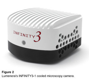 or minutes. The longer the exposure time, the more dark noise you introduce, and that’s where cooling is critical. If you don’t have long exposure times, the uncooled camera may be a better fit.”
“The INFINITY3 also answers a new trend in microscopy, which is the ability to work in both low light and brightfield microscopy applications with the same camera,” continues Graydon. “Today’s researchers may do many types of microscopy, but they don’t want to pay for different cameras for each application. The INFINITY3 can do brightfield through to low light fluorescence. For the lowest light applications, we offer the cooled monochrome INFINITY3 without a Bayer filter. A Bayer filter can absorb as much as 50% of the light thus reducing the sensitivity of a camera. As a result, the INFINITY3 produces a truer, clearer image. The INFINITY ANALYZE software that comes with INFINITY cameras allows microscopists to add color to monochrome low-light images.”
Eyes Wide Shut for Microprocessors
Short wave infrared (SWIR) imaging applications in microprocessor inspection are another area of microscopy that needs high sensitivity to succeed.
“A SWIR microscope is a useful tool for in-process verification for pre-bond and pre-hybridization on critical alignment applications in MEMS (micro-electro mechanical systems), wafer bonding and 3D chip stacking. In post-process operations, it can be used for validation and direct measurement of sub-surface features in silicon, GaAs and other SWIR transmissible materials,” explains Raf Vandersmissen, Chief Executive Officer of sInfraRed, a Xenics company. “In solar cell characterization, scientific grade Si CCD cameras are typically used for luminescence imaging applications. These cameras however have to be cooled significantly to reduce noise and dark current. Moreover, Si CCD based cameras, with a cut-off wavelength at 1100 nm, will only detect the short wavelength tail of the band-to-band luminescence from silicon solar cells at room temperature. By using a SWIR InGaAs camera, you can achieve an order of magnitude enhancement of the measured photon flux. An InGaAs camera is sensitive throughout the entire spectral range in which band-to-band emission from crystalline silicon occurs. Another benefit of using an InGaAs camera is that it is sensitive to an emission band in the spectral range 1400 to 1700 nm. This defect luminescence is linked to the presence of dislocations and is detectable as a broad spectral emission band around 1550 nm at room temperature.”
To optimize photon collection, sInfraRed’s Xeva 1.7 InGaAs cameras have a 30-micron pitch from pixel to pixel and come with optional thermoelectric cooling to further increasing the sensitivity.
Whether the electromagnetic radiation is from the visible spectrum, infrared spectrum, or somewhere in between, machine vision technology has adapted through the use of new architectures and materials to acquire the best possible images for low-light applications. Today, both silicon and compound semiconductor sensors are capable of sensing single photons - the nadir for low-light applications. As these cameras continue to evolve, camera manufacturers will walk the fine line of increasing the size of low-light sensor arrays, using cost effective methods that meet a growing number of low-light machine vision applications.
AIA
AIA - Advancing Vision + Imaging has transformed into the Association for Advancing Automation, the leading global automation trade association of the vision + imaging, robotics, motion control, and industrial AI industries.
Discover how AIA can support your automation journey with their complete range of solutions and expertise.
Visit Company Website
AIA - Advancing Vision + Imaging has transformed into the Association for Advancing Automation, the leading global automation trade association of the vision + imaging, robotics, motion control, and industrial AI industries.