Industry Insights
Designers Say "QuantumFilm" Sensor Promises to Revolutionize Imaging
Today, the machine vision industry depends on charge-coupled device (CCD) and complimentary metal-oxide-semiconductor (CMOS) sensors to collect light and convert photons into electrons and acquire an image of everything from milk containers to automobile engines. These two technologies were initially posited in the 1960s with CCDs gaining greater acceptance because of their higher quality, and use of better-understood semiconductor manufacturing processes. In the 1980s, CMOS sensors started to catch up with the explosion of microprocessors – which use the same manufacturing technology as a CMOS sensor.
Now, the sensor marketplace could be poised for another revolution, thanks to QuantumFilm sensors that can convert nearly 100% of incident photons into electrons.
What is QuantumFilm?
As a general rule, manufacturers make their products cheaper the faster they produce them. Faster processes mean the machine vision cameras have less time to ‘acquire’ an image and avoid image blur caused by an object moving during the few microseconds the sensor is exposed to the light. In response, camera designers must maximize the number of photons they can capture while reducing the electronic ‘noise’ induced by readout electronics that compromise overall sensor efficiency.
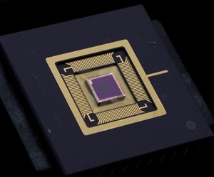
![]()
Image courtesy of InVisage, Inc.
While photographic film has a quantum efficiency (QE) – the ability to convert one photon into one electron - of approximately 10%, traditional CCD designs average 40% to 50%. CMOS sensors can achieve upwards of 80% with backlit designs, but these sensor designs are considerably more expensive than traditional CCD and CMOS sensor designs. The problem is made more difficult as camera customers demand higher spatial resolution sensors for the same price as previous generation cameras. Camera designers can either increase the size of their sensors, reducing the number of sensors they generate from one silicon wafer, or shrink pixel sizes to keep yields high and camera costs low. The smaller the pixels, the fewer incident photons are available, which quickly becomes counterproductive for a high-sensitivity industrial camera.
Furthermore, CCD and CMOS sensor designs do not offer 100% fill factor for each pixel in order to make room for pixel segmentation, amplifiers, and other silicon structures. In response sensor makers may apply a layer of micro lenses over each sensor – one for each pixel – and/or etch the sensor to directly expose the silicon layer and capture additional photons that would normally fall on non-active portions of the sensor. Because QuantumFilm has a separate photoactive layer, it can use the silicon layer as a ‘quantum shutter’ – a critical feature for industrial cameras that need to read all pixels simultaneously.
 |
|
Image courtesy of InVisage, Inc. |
“Read noise is the same as the very best CMOS, which is excellent, but we combine it with nearly 100% quantum efficiency because the fill factor is near 100% as is the absorption,” explains InVisage’s Sargent. “The quantum dot structures reduces crosstalk [between pixels] and we don’t need micro lenses, which makes it easier to match your image sensor with a wider range of optics since you don’t have to worry about the performance of the micro lenses. InVisage also offers a dramatic improvement in dynamic range over traditional CMOS image sensors.”
“Our QuantumFilm is a very dark material,” continues Sargent. “We designed it from scratch for imaging. A few hundred nanometers’ thickness of QuantumFilm is almost completely absorbing across a spectral range that we tune by choosing the size of the quantum dots.”
Pick Your Spectrum
Unlike CCD and CMOS sensors that use silicon as their photoactive layer, quantum dots do not rely solely on the atomic structure of the sensitive material to determine what wavelength of light the material will absorb. In the ultra small world of the quantum dot, it’s not just the atomic structure of the constituent semiconductor that determines what wavelength the quantum dot will absorb, but the size of the quantum dot. As the dot shrinks to a diameter that is smaller than the characteristic wavelength of an electron – known as the Bohr exciton radius - the electron becomes confined inside the dot. Incident photons that are in resonance with the confined electron’s energy levels are absorbed by the semiconductor nanoparticle, which converts them into electron-hole pairs that can separate and captured by InVisage’s CMOS read out circuits.
More to the point, by altering the size of the nanodot, InVisage can select what wavelengths of light the quantum dots – and therefore the QuantumFilm – will absorb. “One of the great things about working with QuantumFilm is that it allows you to look at spectral regions that you cannot conveniently access with silicon,” says Sargent. “While InVisage’s first products will be visible-light sensors, we have proven we can tune down to the ultraviolet, or out to the infrared as long as 1.7 um.”
Initial InVisage sensors will use Bayer filters for color imaging, but the door is open to combine sensing elements containing quantum dots of different sizes and capture portions of a broadband spectrum within the differently-tuned sensing elements.
InVisage will initially target the high-volume smartphone market, where high resolution and high performance are critical factors for a multi-billion dollar industry. According to Sargent, InVisage has partnered with Taiwan’s TSMC, who is now ramping up its production of the single-layer QuantumFilm so that it can be mass produced in conjunction with existing CMOS manufacturing. The first QuantumFilm sensors are expected to sample at the end of this year.
“If the performance is there for both the sensor and the read out circuit – which is hugely important – we’d certainly be interested to hear more about Quantum Film sensors,” says Michael Brown, Chief Technology Officer of PixeLINK (Ottawa, Ontario, Canada).
AIA
AIA - Advancing Vision + Imaging has transformed into the Association for Advancing Automation, the leading global automation trade association of the vision + imaging, robotics, motion control, and industrial AI industries.
Discover how AIA can support your automation journey with their complete range of solutions and expertise.
Visit Company Website
AIA - Advancing Vision + Imaging has transformed into the Association for Advancing Automation, the leading global automation trade association of the vision + imaging, robotics, motion control, and industrial AI industries.